Intel Details Xe GPU- Exascale Chiplet HPC GPU with HBM at 7nm
At the HPC Devcon event, Intel opened up its GPU design called Xe aimed at HPC by Raja Koduri himself. Code name Ponte Vecchio, which we have covered earlier, This GPU will also display the next generation 7nm manufacturing process as well.

The Xe architecture will be a single base architecture that will cover which will be scaled for different segments like HPC, gaming, workstation, etc. For example in mobile segment, the GPU can be stripped to a minimum due to power constraints, HPC can get double precision, AI can be enabled in workstation, gaming GPU can get ray tracing cores etc.
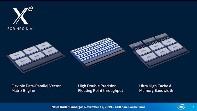
In this conference, Intel rightly focused on HPC related GPU. The GPU will get trio of feature to enable leadership performance:
- Flexible data-parallel vector matrix engine for AI acceleration
- High double precision (FP64) throughput
- High cache and memory bandwidth
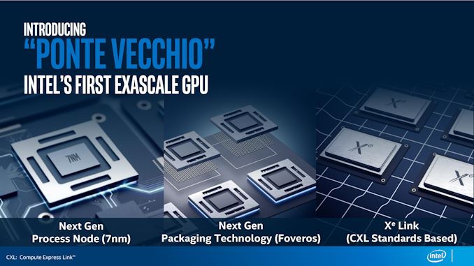
The first output of the above set of features is “Ponte Vecchio”. This is GPU will have
- An exascale GPU design
- Manufactured at 7nm sporting 2x density from 10nm
- Chiplet Technology (MCM design): Ponte Vecchio will use 16 compute chiplet. This is similar to what Nvidia will be aiming with Hopper GPU.
- Foveros and EMIB technology to join chiplets: Forveros technology to interconnect with the Rambo cache which would be shared across several other Xe HPC GPUs. EMIB would be used to connect the HBM memory with the GPUs.
- GPU with GPU will be connected using Compute eXpress Link (CXL) utilising PCIe 5.0 lanes.
What is MCM design?
This is called MutiChip Module. Right now we have a single GPU in a single package, the GPU has to be huge to get more transistors which can be shrunk down with small manufacturing processes. The system identified this system as one GPU. With MCM design there can be multiple GPU in a single package that can work in tandem.
Think of this like AMD’s Chiplet design on CPU side. Where multiple chips are packaged in single die and its like one giant CPU.
There is a limit to how much a GPU can be made larger. Also in one large silicon, if there is a defect, the whole silicon goes to waste. but with small GPUs glued together, any silicon with the defect can be discarded which will be a small wastage. Further, the GPU silicon can be stacked in 3D instead of side by side which can also save space.
What is CXL interconnect link / bus?
It is a high-speed CPU-to-Device and CPU-to-Memory interconnect designed to accelerate data center performance. It allows high speed connection between compute units like CPU and GPU in server segment with high bandwidth.
CXL is designed to be an industry open standard (used by ARM, Nvidia, AMD etc) interface for high-speed communications, as accelerators are increasingly used to complement CPUs in support of emerging applications such as Artificial Intelligence and Machine Learning and thus anyone can use this specification.
What is Foveros packaging?
Foveros packaging technology which is Intel’s new approach to heterogeneous system integration where chips are 3D stacked and allows mix and match of IP blocks with various memory and I/O elements
- Titan Fall(ter): Intel’s Stumble an Analysis - August 5, 2024
- AMDs Radeon Future Looks Bleak After RDNA 5 - May 1, 2024
- Kinect 2- Right time to use A.I. in Nextgen Consoles? - April 30, 2024





When I initially commented I clicked the “Notify me when new comments are added” checkbox
and now each time a comment is added I get four e-mails with
the same comment. Is there any way you can remove me from
that service? Cheers!