AMD announces first multichip MI200 Instinct GPU: 58 billion transistors, 96 TFLOPS @FP64
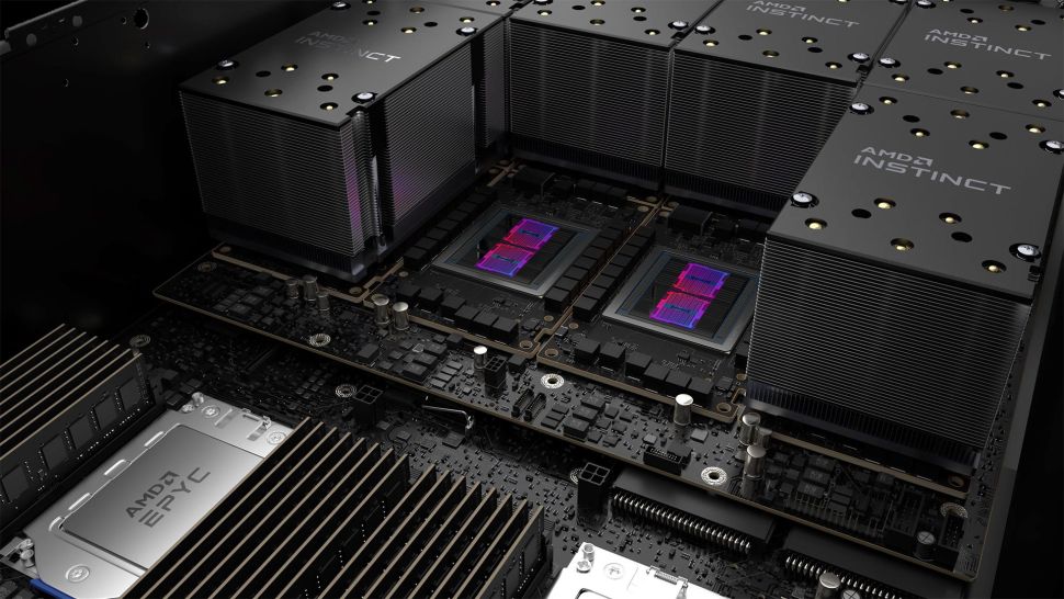
The next gen war has already begun and it has started with AMD announcing its first-ever MCM design GPU called MI200 which is aimed at the data center and will take head-on with Nvidia’s current offering of A100 data center GPU and surpasses its own last offering, the MI100 Instinct GPU, both being monolithic design.
What are MCM and monolithic designs?
before we move further let’s clear this jargon first. Monolithic design is the traditional way of designing GPU where one big chip is designed with all the memory unit and controllers embedded in it. The operating system also perceives it as a single GPU. In an MCM (Multi Chip Module) design is a method of combining two or more GPU chips in one single design. They work in tandem by connecting themselves with a communication fabric (infinity fabric is used here) and the system still perceives it as a single GPU but performance if optimized correctly will go double or n times as per chips.
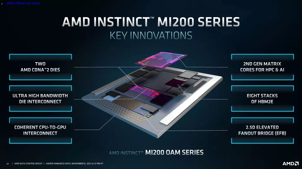
Back to MI200, this is a new design as AMD has never done MCM GPU and is internally calling it CDNA 2 architecture which as it sounds, is an upgrade to MI100 which was based on CDNA architecture. However, this does borrow lots of work gone into Zen CPU design which is already using chiplet design.
AMD’s MI100 vs AMD’s MI200
Just upfront the biggest change is MI100 was monolithic in design which had just one chip inside. MI200 takes it two-notch further with a dual chip inside. Chips on MI200 are communicating with a 3rd gen infinity fabric of 25 Gbps link with a bandwidth of 100GBps (both ways combined). with 8 fabric links, the bandwidth goes up to massive 800 GBps.
MI200 uses TSMC’s 6nm node compared to 7nm node used of MI100
MI200, therefore, is able to clock up to 1.7 GHz driving transistor counts 58.2 billion transistors whereas MI100 was limited to 1.5 GHz and was driving 50 billion transistors.
even though both are using HBM memory, memory bandwidth has increased from 1.2 TBps to 3.2 TBps, all thanks to HBM2e memory and dual chiplet design.
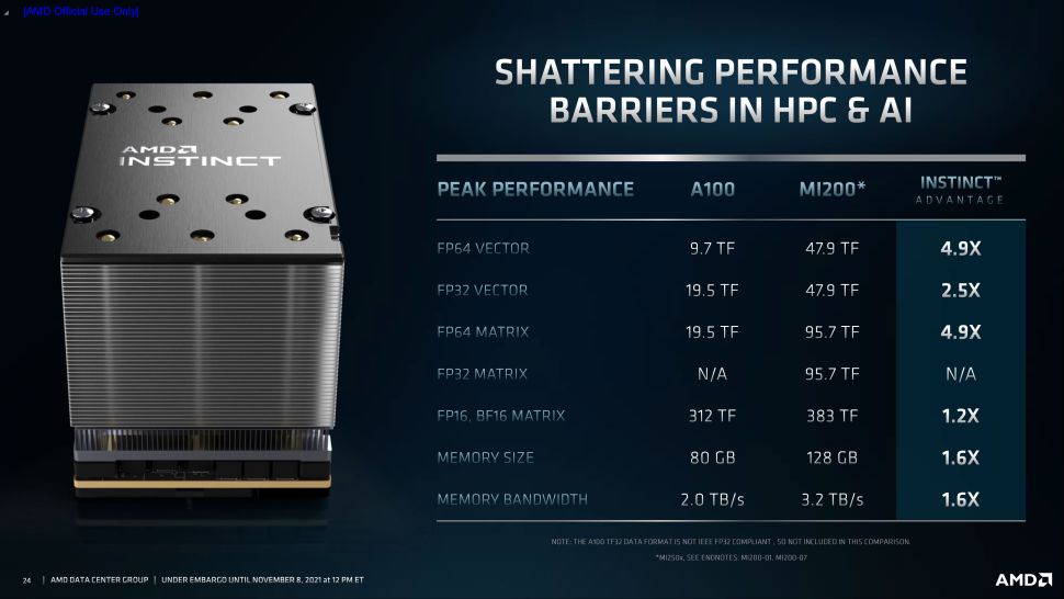
All this has culminated into peak performance of 47.9 TFLOPS at FP64 compared to just 11.54 TFLOPS for MI100. in fact MI200 adds FP64 Matrix support which further increases the performance at 95.7 TFLOPS. FP16 performance is still comparable with MI100 having 184.6 TFLOPS and MI200 having 383 TFLOPS.
AMD’s MI200 vs Nvidia’s A100
Again, the biggest change is A100 was monolithic in design and MI200 is MCM design with a dual chip inside.
MI200 uses TSMC’s 6nm node compared to 7nm node used of A100
MI200, therefore, is driving transistor that counts to 58.2 billion whereas A100 is limited to 54 billion transistors. Thus even when comparing last generation chip by Nvidia, the transistor count difference is not that huge.
Even though both are using HBMe memory, memory bandwidth with a difference from 1.6 TBps in A100 to 3.2 TBps in MI200. Memory size also goes from 80GB in A100 to 128GB in MI200.
All this has culminated into peak performance of 47.9 TFLOPS at FP64 compared to just 9.7 TFLOPS for A100. in fact MI200 adds FP64 Matrix support which further increases the performance at 95.7 TFLOPS. AI100 already has that support which peaked at 19.5 TFLOPS. FP16 performance is still comparable with A100 having 312 TFLOPS and MI200 having 383 TFLOPS.
All in all, with MCM design on hand, AMD has taken its performance level to the next and we sure can hope that this will continue further in the future and MCM unleashes next-generation design. We as can also dream of having MCM design in gaming CPU also which if comes true will mark AMD is first of all the trio of GPU maker to launch MCM gaming GPU.
However, Nvidia is also working on MCM design and time will tell if MI200 will be able to compete with A200 (or whatever Nvidia calls them.

- Titan Fall(ter): Intel’s Stumble an Analysis - August 5, 2024
- AMDs Radeon Future Looks Bleak After RDNA 5 - May 1, 2024
- Kinect 2- Right time to use A.I. in Nextgen Consoles? - April 30, 2024